Overview
This experiment demonstrates the functionality of a basic digital logic circuit called a half-adder. A half-adder is a fundamental building block in digital electronics, used to perform binary addition of two single-bit numbers. The circuit produces two outputs: the Sum (S) and the Carry (C).
The half-adder utilizes two types of logic gates: an XOR gate for the sum and an AND gate for the carry. Understanding this concept is critical for designing more complex arithmetic circuits like full-adders and arithmetic logic units (ALUs).
Components Required
- XOR gate (e.g., 74LS86) - For generating the sum output
- AND gate (e.g., 74LS08) - For generating the carry output
- Resistors (330Ω) - For current limiting
- Power supply - 5V DC for powering the logic gates
- Breadboard - For assembling the circuit
- Connecting wires - For connections
- Multimeter - To measure outputs and verify logic levels
Circuit Diagram
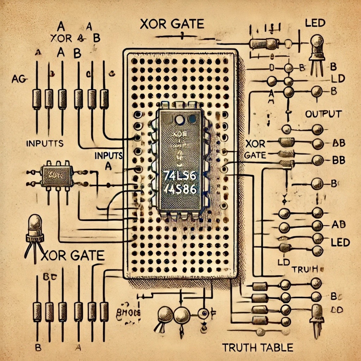
Below is the conceptual representation of a half-adder circuit:
Wiring Instructions:
- Connect input A to the first input of both the XOR gate and the AND gate.
- Connect input B to the second input of both the XOR gate and the AND gate.
- The output of the XOR gate will provide the Sum (S).
- The output of the AND gate will provide the Carry (C).
This simple wiring will implement the half-adder logic, where the Sum (S) is the result of the XOR gate, and the Carry (C) is the result of the AND gate.
Procedure
- Place the XOR and AND gate ICs on the breadboard and connect their power (Vcc) and ground (GND) pins to the 5V DC power supply.
- Connect the two input binary values (A and B) to the input pins of both the XOR and AND gates.
- Use resistors to limit current for any LEDs used as indicators for the outputs.
- Attach LEDs or use a multimeter to observe the outputs:
- The XOR gate will output a HIGH signal (1) if A and B are different, representing the Sum (S).
- The AND gate will output a HIGH signal (1) only if both A and B are HIGH, representing the Carry (C).
- Test the circuit by applying all possible combinations of A and B (00, 01, 10, 11) and verify the outputs.
Expected Result
The half-adder circuit should produce the following output for each combination of inputs:
| Input A | Input B | Sum (S) | Carry (C) |
|---|---|---|---|
| 0 | 0 | 0 | 0 |
| 0 | 1 | 1 | 0 |
| 1 | 0 | 1 | 0 |
| 1 | 1 | 0 | 1 |
Real-World Applications
- Arithmetic Units: Half-adders are used in the design of full-adders and arithmetic logic units (ALUs) in CPUs.
- Digital Signal Processing: Binary addition is essential in data manipulation and processing tasks.
- Educational Projects: Simple circuits like half-adders are often used for teaching basic digital electronics concepts.
Troubleshooting Tips
- Ensure all connections are secure on the breadboard, as loose wires can lead to faulty outputs.
- Verify the power supply voltage is stable and suitable for the logic gates.
- Double-check the pin configuration for the XOR and AND gate ICs from their datasheets to avoid incorrect wiring.
- If the circuit doesn’t work as expected, test individual components like LEDs, gates, and resistors using a multimeter.
Conclusion
This experiment demonstrates the fundamental operation of a half-adder circuit. By understanding the logic behind binary addition and its implementation, you can progress to designing more complex circuits like full-adders, binary multipliers, and integrated digital systems.
